Two-dimensional electron gases (2DEGs) are a fundamental element of modern electronics. Among the various systems capable of hosting them, complex oxide heterostructures stand out. In addition to offering very high electronic mobility, these systems allow for the exploitation of unique properties, such as spin-orbit coupling and strong electronic correlations. These features pave the way for new functionalities, while creating links to fields such as spintronics and photonics. In this context, the ability to manipulate 2DEGs using external stimuli is considered a holy grail. In this study, the researchers demonstrated the instant creation of a 2DEG at the interface between two oxides, where such an electronic state is otherwise absent, using light. This 2DEG disappears just as quickly once the light is turned off. The result is a giant photoconductance effect: under illumination, the electrical conductance is up to five orders of magnitude higher than in the dark! These effects were observed at the interface between thin layers of Nd₁₋ₓSrₓNiO₂ (x = 0, 0.05, and 0.2) and their SrTiO₃ substrate.
To achieve these results, the researchers first epitaxially deposited ultrathin layers of the perovskite Nd₁₋ₓSrₓNiO₃ (x = 0, 0.05, and 0.2) on SrTiO₃ using pulsed laser deposition. Then, a topotactic reduction process allowed them to obtain the infinite-layer phase of Nd₁₋ₓSrₓNiO₂. Transport measurements under ultraviolet and visible light revealed photoconductance effects and their dependence on photon energy. To uncover the microscopic mechanisms responsible for the generation of the 2DEG, the team combined an in-depth study of the interface using transmission electron microscopy (4D-STEM) and electron energy loss spectroscopy (EELS) with advanced density functional theory calculations. They highlighted that the key factors for generating the 2DEG are the structural and electronic reconstructions at the NdNiO₂//SrTiO₃ interface, as well as the presence of an intrinsic interfacial electric field. This field promotes the occupation of the high-mobility Ti-3dxy conduction band by photoexcited electrons, drawing them toward the interface and separating them from the holes left in the Ti valence band. These results are very interesting, both from a fundamental perspective and for their potential applications. On the one hand, they reveal how slight variations in the electronic structure at the interface – whether related to atomic layer terminations, local oxidation states, or temperature – can significantly modulate the confinement and distribution of photo-generated carriers in the interfacial bands. On the other hand, this refined understanding of the underlying microscopic mechanisms opens up promising perspectives for engineering the photo-response of strongly correlated electrons. Among the potential applications, one can consider, for example, the optical control of the superconducting state in infinite-layer nickelates.
The work presented in this article is the result of collaboration between several laboratories in France (LAF, IPCMS, LPS, SOLEIL), Germany (University of Duisburg-Essen), Spain (Universidad Complutense de Madrid), and the United States (University of Florida). This work is part of a broader effort at CNRS, dedicated to manipulating electronic states with light in strongly correlated oxides and their heterostructures, including superconductors, spintronic and electronic materials, within the EIC Pathfinder projects “JOSEPHINE” and “SPINMAT” under the PEPR SPIN program.
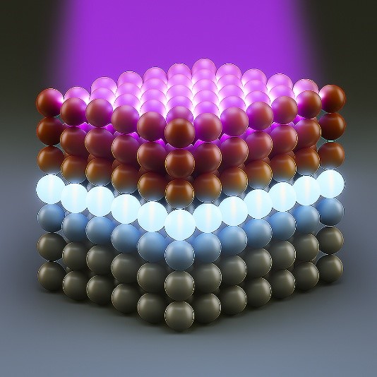
Figure 1: Representation of the photo generation of a two-dimensional electron gas at the interface between two oxides
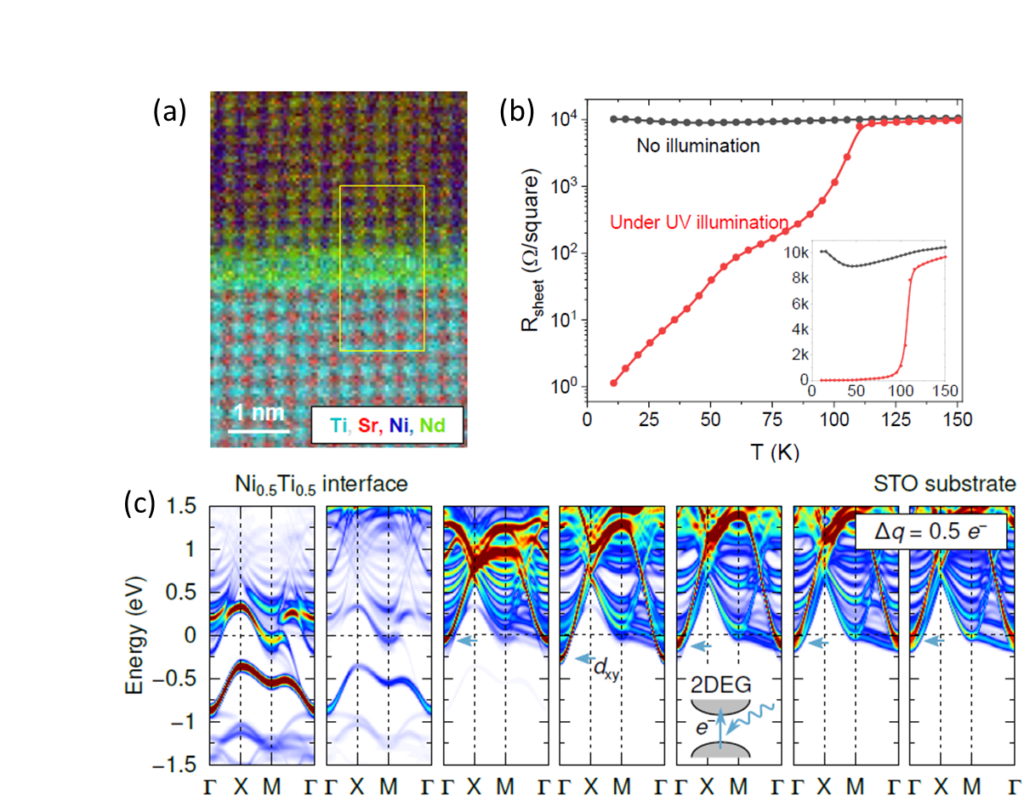
Figure 2 (a) Transmission electron microscopy image combined with electron energy loss spectroscopy of an NdNiO₂//SrTiO₃ heterostructure. (c) Electrical resistance vs. temperature under illumination and in the dark, showing the giant photoconductance effect. (d) Energy bands and Fermi level at the interface and in several atomic planes from it, calculated by density functional theory
Reference : Giant photoconductance at infinite-layer nickelate/SrTiO3 interfaces via an optically induced high-mobility electron gas.
D. Sanchez-Manzano, G. Krieger, A. Raji, B. Geisler, V. Humbert, H. Jaffrès, J. Santamaría, R. Pentcheva, A. Gloter, D. Preziosi et Javier E. Villegas. Nature Materials, le 10 octobre 2025
Contacts :
Javier VILLEGAS, Laboratoire Albert Fert, CNRS, Thales, Université Paris-Saclay (javier.villegas@cnrs-thales.fr)
Daniele PREZIOSI, Institut de Physique et de Chimie des Matériaux de Strasbourg (daniele.preziosi@ipcms.unistra.fr)
Alexandre GLOTER, Laboratoire de Physique de Solides, Université Paris-Saclay (alexandre.gloter@universite-paris-saclay.fr)
You can also read the “Actualité” on CNRS Physique website
Also Read
Official launch of the start-up Lumensium
Scientific Workshop « Electron Microscopy at High Spatial and Temporal Resolution: Current Status and Future Perspectives in Material Characterization »